爱的色放在线观看,国产精品美女一区二区三区,欧美性生交XXXXX久久久,天天做天天爱夜夜爽


免費注冊快速求購


分享
舉報 評價

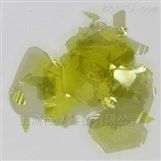
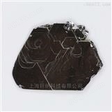
In2S3 crystals 三硫化二銦晶體

參考價面議
具體成交價以合同協議為準

聯系方式:袁經理 查看聯系方式

聯系我們時請說明是儀器網上看到的信息,謝謝!


該廠商其他產品

我也要出現在這里

Gamma layered phase of In2S3 is a direct gap semiconductor with an optical band gap ranging from 2 eV - 3.25 eV.

詳細信息 在線詢價

Gamma layered phase of In2S3 is a direct gap semiconductor with an optical band gap ranging from 2 eV - 3.25 eV. It's fundamental band gap nature (direct vs indirect) and its value have been much debaded in the field and remains open ended. In2S3 is particular attractive semiconductor for photoelectrochemical, solar cell, and photonic applications. Typical crystal sizes range in few-mm in size and each order contains 5-7 pieces of In2S3 crystals. The crystals appear layered but is harder to exfoliate compared to molybdenum disulfide. Thus, we recommend using highly adhesive tapes, ultrasonic exfoliation, or other methods to yield atomically thin sheets.

上海巨納科技有限公司

|

手機:13761090949

聯系人:袁經理

電話:86-21-31255909

傳真:86-21-60852363

(聯系我時,請說明是在儀器網上看到的,謝謝!)

同類產品推薦


提示

×

*您想獲取產品的資料:

以上可多選,勾選其他,可自行輸入要求

個人信息: