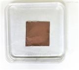
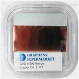
爱的色放在线观看,国产精品美女一区二区三区,欧美性生交XXXXX久久久,天天做天天爱夜夜爽


免費(fèi)注冊(cè)快速求購(gòu)


分享
舉報(bào) 評(píng)價(jià)

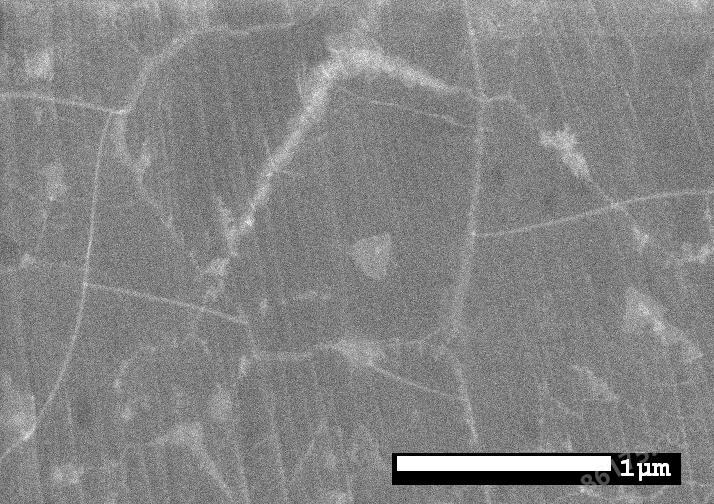
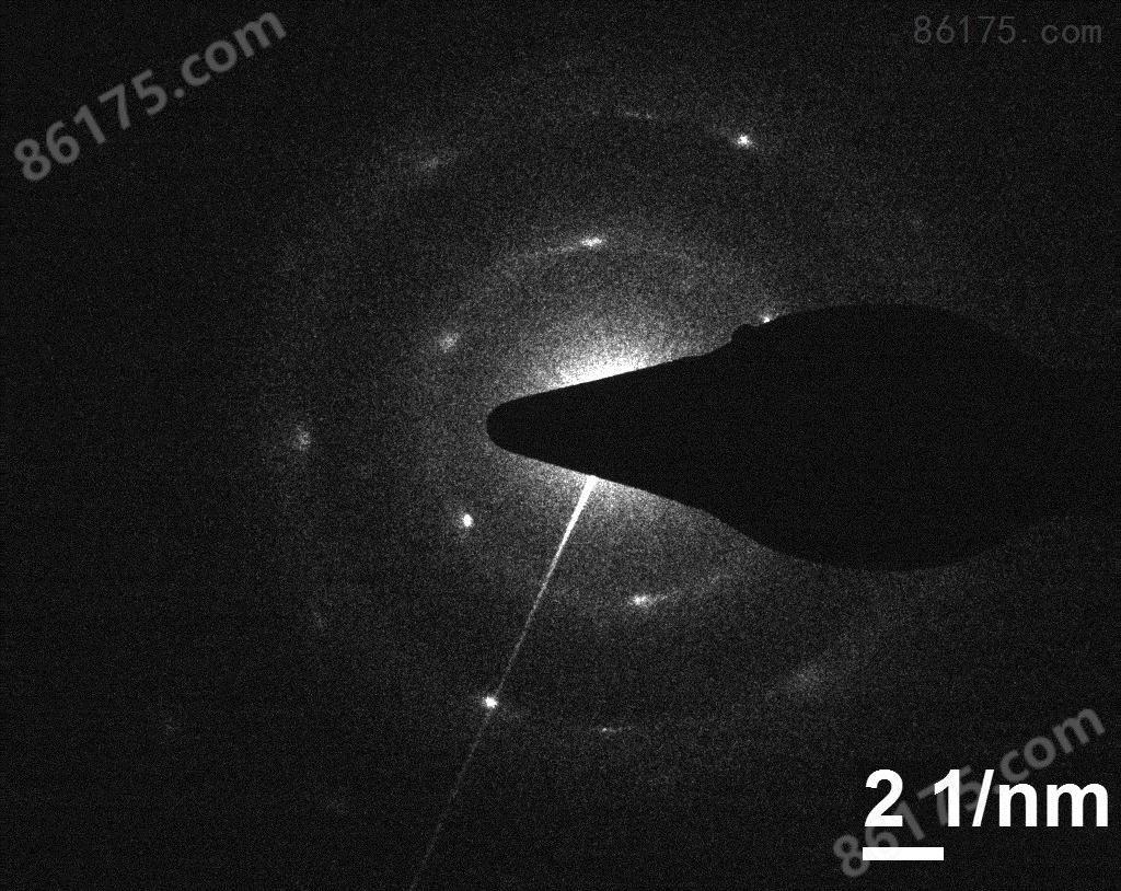
基于銅基的單層氮化硼薄膜(5*2.5cm)

參考價(jià)面議
具體成交價(jià)以合同協(xié)議為準(zhǔn)
  • 公司名稱 上海巨納科技有限公司
  • 品牌
  • 型號(hào)
  • 所在地
  • 廠商性質(zhì) 經(jīng)銷商
  • 更新時(shí)間 2020/12/26 13:52:17
  • 訪問(wèn)次數(shù) 316

聯(lián)系方式:袁經(jīng)理 查看聯(lián)系方式

聯(lián)系我們時(shí)請(qǐng)說(shuō)明是儀器網(wǎng)上看到的信息,謝謝!


該廠商其他產(chǎn)品

我也要出現(xiàn)在這里

Single layer h-BN (Boron Nitride) film grown in copper foil.h-BN is an insulator with a direct band gap of 5.97 eV. Due to its strong covalent sp2 bonds in the plane, the in-plane mechanical strength

詳細(xì)信息 在線詢價(jià)

Single layer h-BN (Boron Nitride) film grown in copper foil.

h-BN is an insulator with a direct band gap of 5.97 eV. Due to its strong covalent sp2 bonds in the plane, the in-plane mechanical strength and thermal conductivity of h-BN has been reported to be close to that of graphene. h-BN has an even higher chemical stability than graphene; it can be stable in air up to 1000 °C (in contrast, for graphene the corresponding temperature is 600 °C).

During Chemical Vapor Deposition, BN is grown on both sides of the copper foil

Specifications:

Close to complete coverage (90-95%), with some minor holes

Thickness of the copper foil is 20 microns

High crystalline quality, see SAD (Selected area [electron] diffraction) data

Quality is confirmed by TEM. TEM shows perfect hexagonal structure.

TEM image of perfect hexagonal structure

On SEM image (below), BN is seen as wrinkles on top of the copper foil.

SAD data of h-BN

If transferred onto an SiO2 substrate, the BN film may be seen as a white film. However, it is difficult to recognize the BN film on copper using a microscope.

Absorbance data BN on copper

上海巨納科技有限公司

|

手機(jī):13761090949

聯(lián)系人:袁經(jīng)理

電話:86-21-31255909

傳真:86-21-60852363

(聯(lián)系我時(shí),請(qǐng)說(shuō)明是在儀器網(wǎng)上看到的,謝謝!)

同類產(chǎn)品推薦


提示

×

*您想獲取產(chǎn)品的資料:

以上可多選,勾選其他,可自行輸入要求

個(gè)人信息: